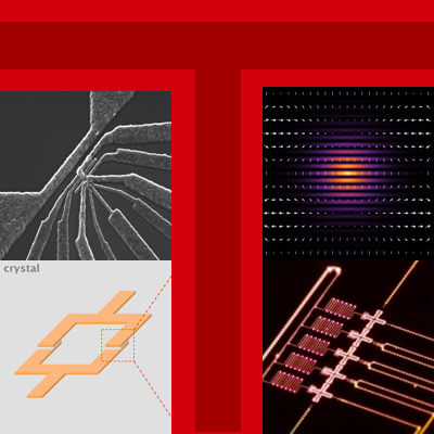
We propose a non-destructive means of characterizing a semiconductor wafer via measuring the parameters of an induced quantum dot on the material system of interest with a separate probe chip that can also house the measurement circuitry. We show that a single wire can create the dot, determine if an electron is present, and be used to measure critical device parameters. Adding more wires enables more complicated (potentially multi-dot) systems and measurements. As one application for this concept, we consider a silicon metal-oxide-semiconductor and silicon/silicon-germanium quantum dot qubits relevant to quantum computing and show how to measure low-lying excited states (so-called “valley” states). This approach provides an alternative method for the characterization of parameters that are critical for various semiconductor-based quantum dot devices without fabricating such devices.
Induced quantum dot probe for material characterization (aip.scitation.org)
Scilight: Proposed probe chip a potential shortcut for quantum device manufacturing cycle
Alternative method of characterizing semiconductor material properties with a separate probe chip that induces quantum dots could speed optimization of quantum dot spin qubits.